Digital Thermometer and Thermostat
_______________________________________________________________________________________ 3
Note 1: All voltages are referenced to ground.
Note 2: Internal heating caused by O.S. loading causes the DS7505 to read approximately 0.5?/SPAN>C higher if O.S. is sinking the
max-rated current.
Note 3: Specified in 12-bit conversion mode. Quantization error must be considered when converting in lower resolutions.
Note 4: I
DD
specified with O.S. pin open.
Note 5: I
DD
specified with V
DD
at 3.0V and SDA, SCL = 3.0V, T
A
= -55癈 to +85癈.
Note 6: I
DD
specified with A0, A1, A2 = 0V or V
DD
.
Note 7: V
DD
must be > 2.0V.
Note 8: E
2
Copy occurs at +25癈.
Note 9: See the timing diagram (Figure 1). All timing is referenced to 0.9 x V
DD
and 0.1 x V
DD
.
Note 10: After this period, the first clock pulse is generated.
Note 11: The DS7505 provides an internal hold time of at least 75ns on the SDA signal to bridge the undefined region of SCLs
falling edge.
Note 12: For example, if C
B
= 300pF, then t
R(MIN)
= t
F(MIN)
= 50ns.
Note 13: This timeout applies only when the DS7505 is holding SDA low. Other devices can hold SDA low indefinitely and the
DS7505 does not reset.
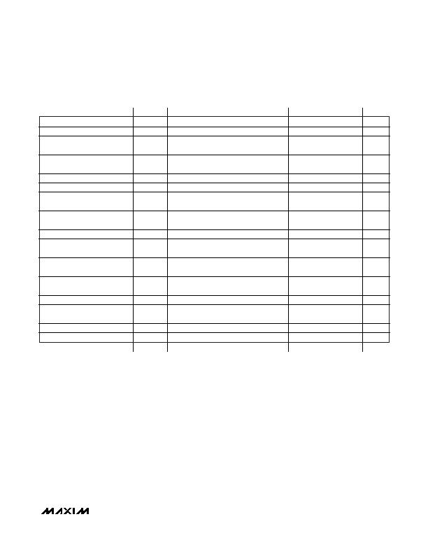
AC ELECTRICAL CHARACTERISTICS (continued)
(1.7V d V
DD
d 3.7V, T
A
= -55癈 to +125癈, unless otherwise noted.)
PARAMETER
SYMBOL
CONDITIONS
MIN
TYP
MAX
UNITS
EEPROM Data Retention
t
EEDR
-40癈 to +125癈 (Note 8)
10
Years
Bus Free Time Between a STOP
and START Condition
t
BUF
(Note 9)
1.3
約
START and Repeated START
Hold Time from Falling SCL
t
HD:STA
(Notes 9, 10)
600
ns
Low Period of SCL
t
LOW
(Note 9)
1.3
約
High Period of SCL
t
HIGH
(Note 9)
0.6
約
Repeated START Condition
Setup Time to Rising SCL
t
SU:STA
(Note 9)
600
ns
Data-Out Hold Time from Falling
SCL
t
HD:DAT
(Notes 9, 11)
0
0.9
約
Data-In Setup Time to Rising
t
SU:DAT
(Note 9)
100
ns
Rise Time of SDA and SCL
(Receive)
t
R
(Notes 9, 12)
20 +
0.1C
B
300
ns
Fall Time of SDA and SCL
(Receive)
t
F
(Notes 9, 12)
20 +
0.1C
B
300
ns
Spike Suppression Filter Time
(Deglitch Filter)
t
SS
0
50
ns
STOP Setup Time to Rising SCL
t
SU:STO
(Note 9)
600
ns
Capacitive Load for Each Bus
Line
C
B
400
pF
Input Capacitance
C
I
5
pF
Serial Interface Reset Time
t
TIMEOUT
SDA time low (Note 13)
75
325
ms
发布紧急采购,3分钟左右您将得到回复。
相关PDF资料
DS75LVU+T&R
IC SENSOR TEMP DIGITAL 8MSOP
DS75LXS+
IC THERMOMETER/STAT DIG 8-SOIC
DS75U+T&R
IC THERMOMETER/STAT DIG 8-MSOP
FAN4010IL6X_F113
IC CURRENT SENSE 0.2% 6MLP
FAN5069EMTCX
IC REG DL BCK/LINEAR 16TSSOP
HIP1011BCB-T
IC CTRLR HOT PLUG PCI 16-SOIC
HIP1020CK-T
IC CTRLR HOT PLUG SOT23-5
HIP6018BCBZ-T
IC REG TRPL BCK/LINEAR 24-SOIC
相关代理商/技术参数
DS7505UR
制造商:MAXIM 制造商全称:Maxim Integrated Products 功能描述:Digital Thermometer and Thermostat
DS7505UT
制造商:MAXIM 制造商全称:Maxim Integrated Products 功能描述:Digital Thermometer and Thermostat
DS75-08B
功能描述:整流器 75 Amps 800V RoHS:否 制造商:Vishay Semiconductors 产品:Standard Recovery Rectifiers 配置: 反向电压:100 V 正向电压下降: 恢复时间:1.2 us 正向连续电流:2 A 最大浪涌电流:35 A 反向电流 IR:5 uA 安装风格:SMD/SMT 封装 / 箱体:DO-221AC 封装:Reel
DS750PED-3
功能描述:线性和开关式电源 12V output 750W Platinum RoHS:否 制造商:TDK-Lambda 产品:Switching Supplies 开放式框架/封闭式:Enclosed 输出功率额定值:800 W 输入电压:85 VAC to 265 VAC 输出端数量:1 输出电压(通道 1):20 V 输出电流(通道 1):40 A 商用/医用: 输出电压(通道 2): 输出电流(通道 2): 安装风格:Rack 长度: 宽度: 高度:
DS750PED-3-001
制造商:Emerson Network Power - Embedded Power 功能描述:12V OUTPUT, 750W 1U X 3.4 X 7.8 PLATINUM WITH REVERSE AIR - Bulk 制造商:ARTESYN EMBEDDED TECHNOLOGIES 功能描述:AC/DC CONVERTER 12V 12V 750W 制造商:Emerson Embedded Power 功能描述:AC/DC CONVERTER 12V 12V 750W 制造商:Emerson Network Power - Embedded Power 功能描述:12V output, 750W 1U x 3.4 x 7.8 Platinum with reverse air
DS750PED-3-402
制造商:Emerson Network Power - Embedded Power 功能描述:- Bulk
DS750PED-3-403
制造商:Emerson Network Power - Embedded Power 功能描述:12V OUTPUT, 750W 1U X 3.4 X 7.8 PLATINUM WITH REVERSE AIR - Bulk
DS75107
制造商:NSC 制造商全称:National Semiconductor 功能描述:Dual Line Receiver
